Welcome to my circuit-verse!
You will find some cool projects down below


Scroll down to discover some interesting circuits


Portfolio 1: 2-bit Multiplier


This is a general schematic of how a 2-bit unsigned multiplier should work. The circuit multiplies two positive numbers (A1A0 and B1B0) ranging from 0 to 3.
The first step is multiplying the first two LSBs (least significant bits), A0 and B0, using an AND gate and the product is sent directly to the first LED, the LSB of the output LEDs.
The next step is multiplying A1 by B0 and A0 by B1, using an AND gate for each, then feeding the outputs to an XOR gate. The job of the XOR gate is to 'add' the two
numbers together then send the result to the second output LED. Those outputs that went into the XOR gate will be fed into an AND gate to account for a possible carry-out.
The third step is multiplying A1 by B1 to get the last product term and feed it into a second XOR gate along with the carry-out to get a result for our third output LED.
The final step is to plug the product of
A1 and B1 into an AND gate along with the carry-out to account for a second carry-out term and assigning it to the fourth output LED.
Output terms:
First output term: A0B0 Third output term: [(A1B0)(A0B1)] ⊕ A1B1
Second output term: A1B0 ⊕ A0B1 Fourth output term: (A1B0)(A0B1)(A1B1)
Portfolio 2: Odd Parity Generator/Checker
Click on the image to view the simulation:
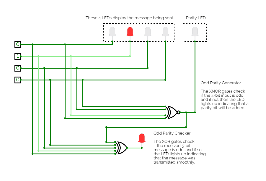
When messages are transmitted in the form of digital signals, there is this tendency for some bits to flip, change from high to low, or vice versa. In the pioneering age of digital signal transmission, one technique utilized to ensure no data was lost was to check for parity. By adding one parity bit either to the beginning or the end of the message, which could be any number of bits in length, the receiving party can discern the
reliability of the message. Both the transmitting party and the receiving party would have to agree on the parity logic beforehand, otherwise, the technique would not work. Here I have chosen to design an odd parity generator and checker.
Portfolio 3: Asynchronous Ripple Counter [Clock]

Digital clocks are all around us, but have you ever wondered what goes into building one? I decided to give it a go. The main logic used in this circuit is asynchronous ripple counters. The circuit utilizes a system of flip-flops, a digital logic chip typically used as counters, to increment the clock digits. The type does not matter, but I used JK flip-flops in my design. Each digit requires an n number of flip-flops to loop from zero to the highest
number needed less than 2^n. For example, the counter required to display the first digit of the seconds and minutes is a decade counter to loop from zero to nine. The number 9 is less than 2^4, or 16; therefore, requiring four flip-flops. For the second digit of the seconds and minutes we need three flip-flops to loop through the numbers zero to five since five is less
than 2^3, or 8.
The inputs of all flip-flops, J and K, should be connected to VCC (power source). The Q output of the flip-flips would go into a BCD to 7-segment display decoder to display the digits on a 7-segment display. The question arises, how do we reset the counters so that they do not exceed the maximum value of 9 or 5? For the decade counter, the output from the second and the fourth (MSB) chips should connect to a NAND gate feeding it into the asynchronous RESET pins of the JK flip-flops. The reasoning behind this logic is that when the flip-flops output the number 10 in binary [1010], the MSB and the second digit act as
the trigger to reset to zero [0000]. As for the 3-chip counter, the second and third (MSB) chips should connect to a NAND gate feeding it into the asynchronous RESET pins. The reasoning is similar to the decade counter: reset the flip-flops to zero when they hit 6 [110].
Great, problem solved, or is it? How do we connect all these flip-flops in a uniform, functioning system? Simply enough, we need a triggering signal to the clock pin of every flip-flop. For the very first counter, connect an oscillating signal to the clock pin of the first flip-flop (LSB) by utilizing a function generator or the like. For the rest of the flip-flops in the set, connect the output (Q) of the preceding flip-flop to the clock pin of the next one. The same goes for every set of flip-flops, excluding the first in each. For those, connect the same inputs that went into the NAND gate into an AND gate and feed the latter's output into the clock pin of the first flip-flop of the succeeding counter.
Portfolio 4: EPROM
Student Data
Click on the image to view the simulation:
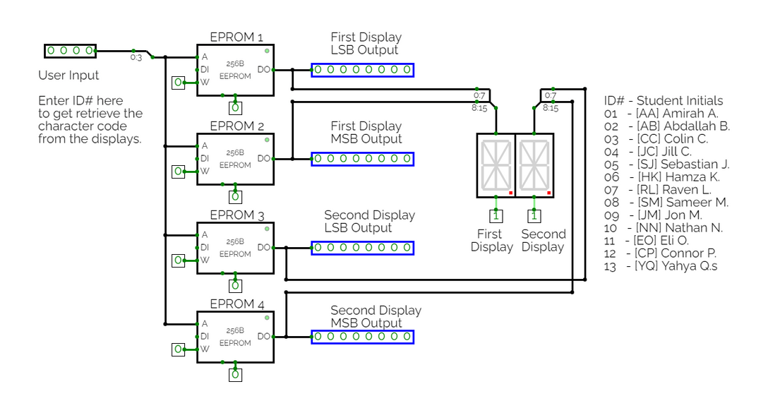
Accessing student data has been simplified using EPROMs and 16-segment displays. The idea behind using an EPROM is that it can store large amounts of data that can be accessed easily simply by invoking the desired address line. The inspiration for this project is the invention of the computer, which can take keyboard input and display characters on a screen. Table 1 reveals the data programmed into the EPROMs. Each row contains the
data stored in an EPROM. These values are in decimal notation derived using the character code table. The character code table was constructed through trial and error and with the help of an online resource [link down below].
Table 1
EPROM Programming Logic
Address Row | 0 1 2 3 4 5 6 7 8 9 10 11 12 13
|------------------------------------------------------------------
EPROM 1 Data | 0 192 192 0 0 192 192 196 192 0 36 128 0 192
EPROM 2 Data | 0 243 243 207 62 221 51 227 221 62 51 207 207 61
EPROM 3 Data | 0 192 82 0 0 0 140 0 40 40 36 0 192 4
EPROM 4 Data | 0 243 252 207 207 62 3 15 51 51 51 255 227 255
EPROM Character Code Table
A B C D E F G H I J K L M N O P Q R S T U V W X Y Z
--------------------------------------------------------------------------------------------------------
192 82 0 18 128 128 64 192 18 0 140 0 40 36 192 4 196 192 18 0 9 5 45 192 9
243 252 207 252 207 195 223 51 204 62 3 15 51 51 255 227 255 227 221 192 63 3 51 0 61 204
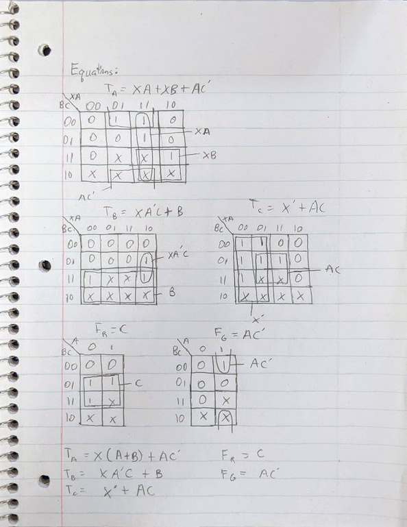
Portfolio 5: FSM
Guess the Sequence Game
Click on the image to view the simulation:
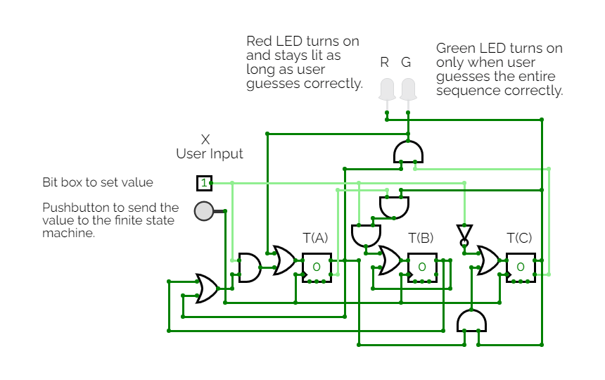
Who doesn't like playing games? That's the motivation for building this finite-state machine that lets you play a guess-the-sequence game. To play, simply toggle the input box to choose a zero or a one, then click the pushbutton to send that value to the finite state machine. The red LED illuminates as long as the input sequence is on track. An affirmative green LED illuminates once the player enters the correct sequence of bits.
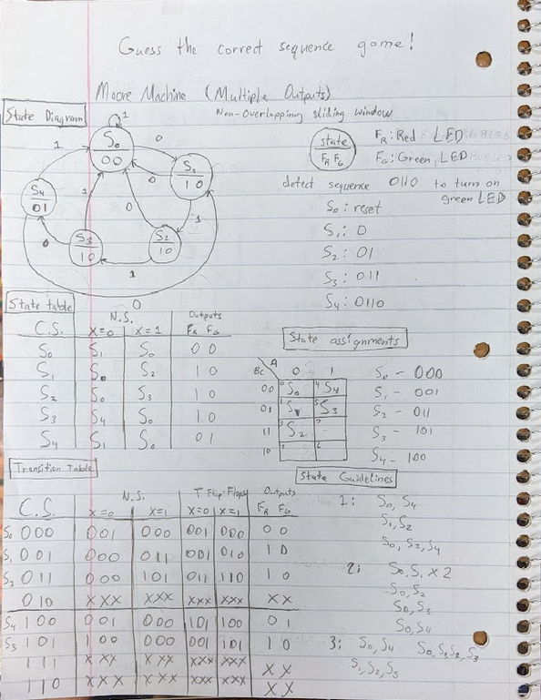
These two pages show the process used to build the finite state machine.
Portfolio 6: Register
Guess the 8-bit Number
Click on the image to view the simulation:
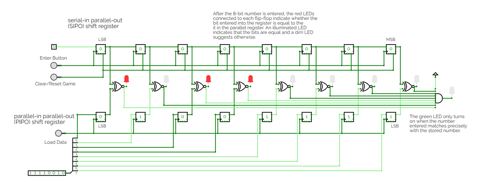
Who doesn't like playing even more games? Here's another neat circuit that utilizes two registers to store data entered by the player and data loaded beforehand, either randomly or by another party. The registers are made up of 8 D flip-flops, each. The bits entered by the player are compared one by one against the bits in the other parallel register. Red LEDs light up, indicating that the value stored in the two corresponding flip-flops match. The player must correctly enter all 8 bits for the green LED to light up.
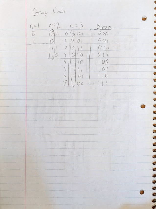
Portfolio 7: Encoder & Decoder - Binary to Gray Code Conversion
Click on the image to view the simulation:
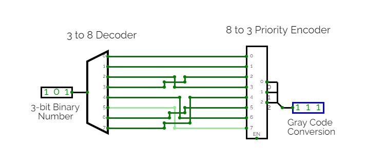
This circuit although seemingly simple introduces a very important concept: switching. Decoders and encoders have been in use for a very long time mainly in the field of communications, but they are also useful in other areas of engineering. I would like to focus on a specific style of binary ordering called gray code. Gray code was conceived by a
a physicist named Frank Gray. The idea behind this code is to flip only one bit, or switch, at a time. This is extremely convenient in telecommunications since flipping multiple switches concurrently does not always result in smooth transmission and may incur malfunctioning of machinery. The world of engineering never ceases to enhance and better itself especially with rising technology.